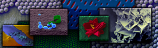
Scanning electron microscope (SEM)
In a scanning electron microscope an electron beam is scanned over the surface of a sample (scanning). The irradiating electrons interact primarily with the sample in the so called interaction volume (figure 2). The Dimension of this volume depends on parameters like the acceleration voltage, the density and the mean atomic number of the sample. The live and still SEM-images are generated from detecting secondary electrons and backscattered electrons. Between detectors the composition of detected electrons varies.

The inlens detector is perpendicular to the sample surface in the electro-optical path. This implies that it can only be used efficiently at low voltages up to 20 kV. In this range the suction of the so called beambooster has a very high yield of electrons. This allows a faster and gentler image generation comparing it with other detectors, especially at very low voltages. Its almost pure detections of secondary electrons allows a very close to the surface image that contains only little information from the bulk phase.
At first the name won’t let you suspect it, but the SE2 detector captures a combination of secondary (SE) and back-scattered (BE) electrons. Compared to the inles detector the image information originates from a greater average sample depth. The SE2 detector distinguishes itself from other detectors because of it’s position inside the machine. By his side mounting to the chamber wall, it gives much better topographical information than other detectors. The lower yield of electrons can be compensated by tilting the sample.
To meet the requirements of radiation-sensitive samples as well as the requirements of X-ray analytics, the NEON® 40 allows many options. Low voltage (0.1 to 5 kV) allows especially near surface images which are very low energetic and gentle. For analytical purposes the accelerating voltage can be increased up to 30 kV. Different apertures, different scanning methods and even an additional modulation of the electron optics (high current mode) extend the variety of intensities.
Besides the pure observation of the surface, different sample preparations offer the view into the sample beneath its surface: The cryofracture, the cross section and of course the FIB technology (see next section).
| specification | NEON® 40 |
| SEM resolution | 1,1 nm @ 20 kV 2,5 nm @ 1 kV |
| SEM probe current | 4 pA - 20 nA |
| SEM acceleration voltage | 0,1 - 30 kV |
| SEM emitter | Schottky field emitter |
Focused Ion Beam (FIB)

More than just a superficial glance: With the Focused Ion Beam (FIB) material can be removed. Making it possible to reveal hidden structures. The ion beam consisting of heavy gallium ions can be understood as a "nanoscopic sandblast" (figure 3). The intensities can be adjusted over a wide range, allowing to change between fast and fine cuts.
| specification | NEON® 40 |
| FIB resolution | 7 nm @ 30 kV granted by the manufacturer, 5 nm possible |
| FIB probe current | 1 pA - 50 nA |
| FIB acceleration voltage | 2 - 30 kV |
| FIB emitter | Ga liquid metal ion source (LMIS) |
| Gas injection system (GIS) | 5 gases for selective etching, enhanced etching, material deposition, insulator deposition |
The combination of FIB and SEM adds up to an instrument, which can remove nanoscopically material and can show the sectional area. At low FIB currents the section can be observed even live by SEM.
 pure scanning electron devices can detect only near-surface structures; b) FIB serial sectioning allows the detection of structures in layers below the surface.")


Gas injection system (GIS)
In addition to the gallium emitter, a gas injection needle block is installed in the device. By injecting the gas near the surface the gallium ion beam can be varied in its effect. The gases are used for...
- selective etching,
- enhanced etching,
- material deposition and
- insulator deposition.
Energy dispersive X-ray spectroscopy (EDX)
By measuring the characteristic X-ray radiation with an additional built-in EDX device (Thermo Fisher Scientific Ultra Dry) it is possible to determinate the elements, macroscopic sample volumes are made of.
Because of the electron bombardment electrons get knocked out of nuclear near shells (fig. 8 a). The resulting gaps are unstable and will fill with electrons from higher shells (fig. 8 b). These electrons fall to a lower level of energy and therefore lose energy. This energy difference is released in form of X-ray quanta (among others) and is characteristic for each transition. Depending on the bond to the nucleus, the energy levels vary, generating a characteristic X-ray spectrum for each element. The minimum voltage, which needs to be applied, depends on the chemical elements and has to be selected high for unknown chemical compositions.
 An electron is kicked out; b) The energy reduction of the electron leads to the release of X-ray radiation.")
The interaction volume, in which the X-ray radiation is produced, is shown in figure 2. The penetration depth depend on the acceleration voltage and the density of the examined sample. A rule of thumb is 1 µm. A lowering to much smaller values is work-intensive to physically impossible.
There are different methods for detecting:
 representation in the software from Thermo Electron b) view in Microsoft Excel.")
- Spectrum: The visible range of the SEM image is used for the determination of the EDX spectrum (fig. 9 a). An access to the raw data is possible. This data can also be imported into spreadhsheet programs (fig. 9 b).
- Point & Shoot: The Point & Shoot mode can create spectras, whose ranges are freely selectable within the SEM image. In addition to the specification of a point (expansion corresponds to the interaction volume), also circle, rectangle and polygones of any kind are possible (of course always considering the interaction volume).

- Linescan: With a linescan the distribution of elements along a line can be represented graphically (fig. 10).
, silicon (green), iron (yellow) und copper (blue) inside an aluminum alloy.")
- Mapping: The Mapping allows a descriptive overview of the element distribution. The colors are arbitrary and can be superimposed on the grey-scale image (fig. 11). However, clearer and more detailed is the representation in separate graphics (fig. 12). Behind each pixel inside the distribution image lays an individual spectra (speactral imaging). Beside those distribution images by counts it is possible to convert them to atomic or mass percent. In addtion this enables the subsequent extraction of spectra and linescans. Spectra, linescans as well as distribution images can be exported and saved graphically as well as on data level. This enables further data processing in external programmes.
 a) grey image (SEM), b) aluminum, c) silicon, d) copper, e) iron, f) oxygen.")