Setup for Infrared microscopy, IRRAS, ATR, and discrete-modulation FTIR
This setup features a Bruker Vertex 70 spectrometer on the left that is coupled to a Hyperion 1000 microscope. This enables IR spectroscopic investigations on defined spots on the sample surface with dimensions down to 20 µm. These measurements can be conducted in transmission, perpendicular reflexion, gracing-incidence reflexion (83°), and attenuated total reflextion (ATR) geometry.
The other end of the IR spectrometer is coupled to a plasma cell, in which atmospheric and low-pressure plasmas can be generated. In this cell, complementary IRRAS (with discrete modulation of light polarization), OES, SKP, and QCM measurements can be performed in-situ.
Setup for polarization modulated infrared reflection-Absorption spectroscopy (PM-IRRAS)
Infrared reflexion absorption spectroscopy (IRRAS) under variable angle of incidence (13-83°) is used for the analysis of thin films. At the heart of the spectrometer is a photoelastic modulator, which enables investigations of molecular monolayers on metallic surfaces via PM-IRRAS. Furthermore, we also employ a diffuse reflexion (DRIFT) cell for the investigation of single crystals and strongly scattering samples.
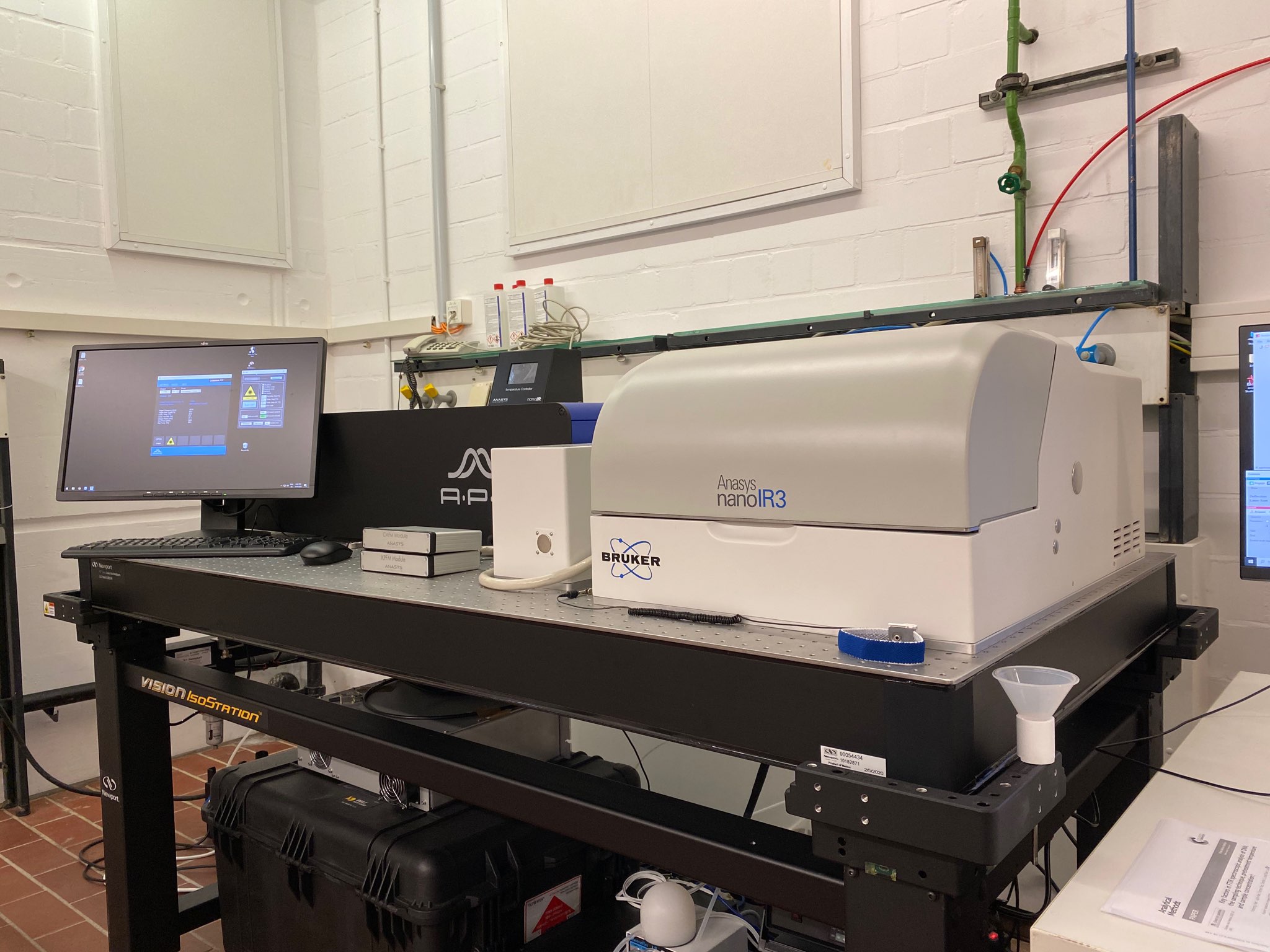
Infrared scattering scanning near field optical microscope
The Anasys NanoIR3s is based on an atomic force microscope (AFM) equipped with an addtional IR laser. It thus provides information on the IR absorption of the surface materials at a lateral resolution of a few nanometers. In the photothermal mode, the thermal expansion of the sample surface underneath the AFM tip upon irradiation with an IR laser pulse is detected by a deflection of the AFM cantilever. This signal can be used to generate a FTIR spectrum or an IR map of the sample surface. In the latter case, the surface topography is being recorded in parallel to the local photothermal expansion at a fixed IR wavelength. This mode is ideal for thin films 20 - 500 nm in thickness and allows to collect chemical information in the wavenumber range 800 - 2000 cm-1. Furthermure, the NanoIR3s is also equipped with an IR scattering scanning near filed optical microscopy (sSNOM) mode, which can be used to characterize inorganic materials with low thermal expansion and optically active materials such as plasmonic nanostructures. All these measurements can be conducted under temperature and humidity control and complemented by electrical surface charectarization using conducting AFM and SKPFM.
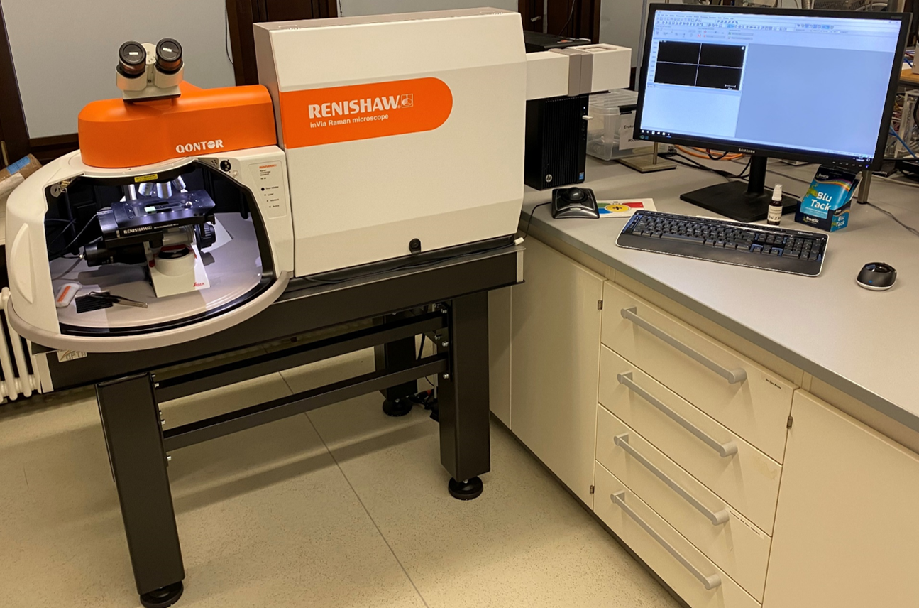
Raman Imaging Spectroscopy
The Raman Imaging Spectrometer is a modular setup consisting of a Renishaw In Via Raman Spectroscope and a Leica DM 2500 M microscope. Raman scattering can be variably excited by an Ar laser (633nm) or a Nd:YAG laser (532nm), and detected by a highly sensitive, ultra-low noise RenCam CCD detector. The microscope uses N PLAN objectives with 5x, 10x, 20x, 50x, and 100x magnification, plus a 63x immersion objective and a 50x long distance objective. Measurement modes include confocal and non-confocal spectral measurements, surface and 3D mappings with a maximum lateral resolution of 500 nm. In addition, the Raman spectrometer can also be used as a fluorescence spectrometer.


